Nanofabrication cleanroom research
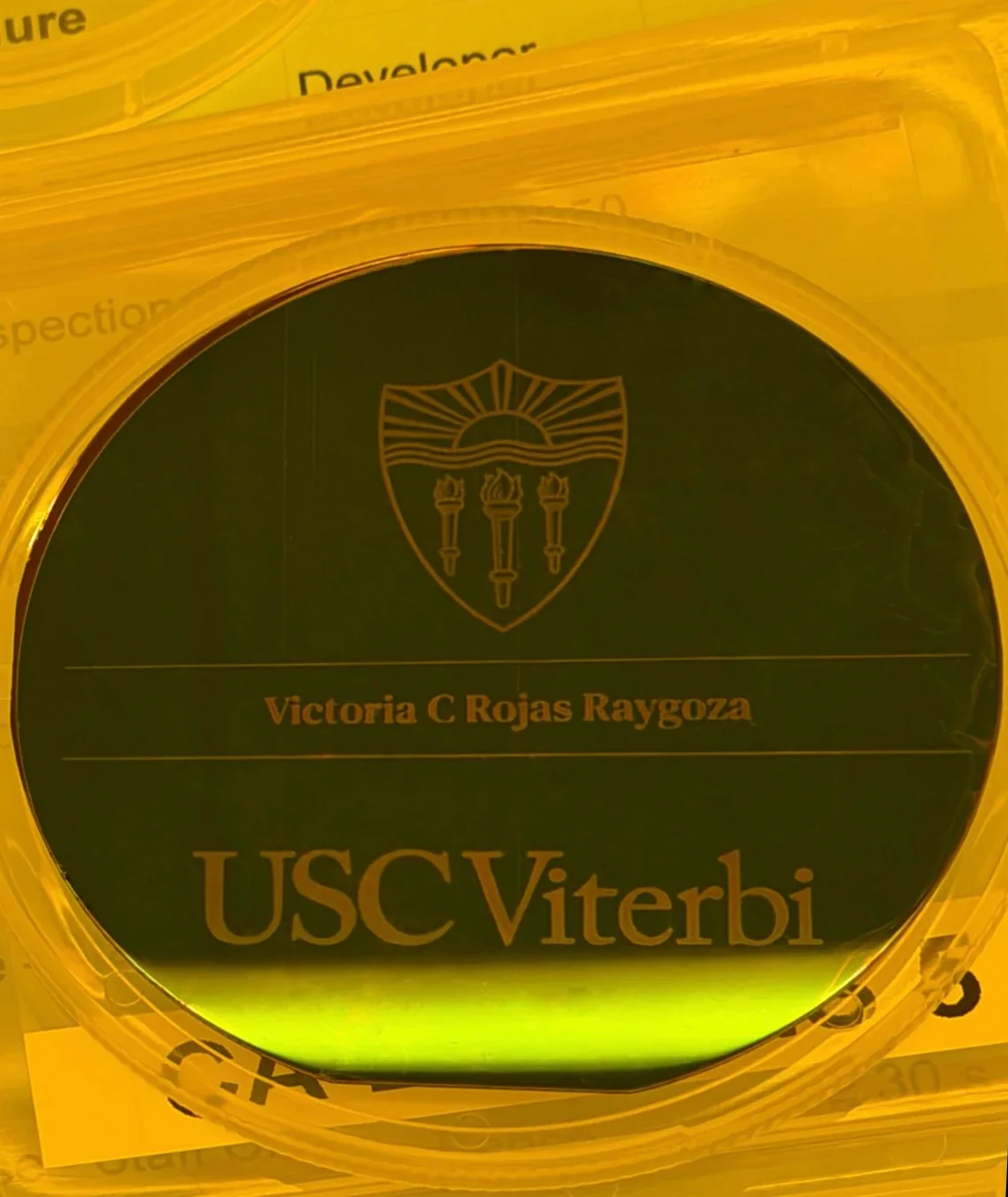
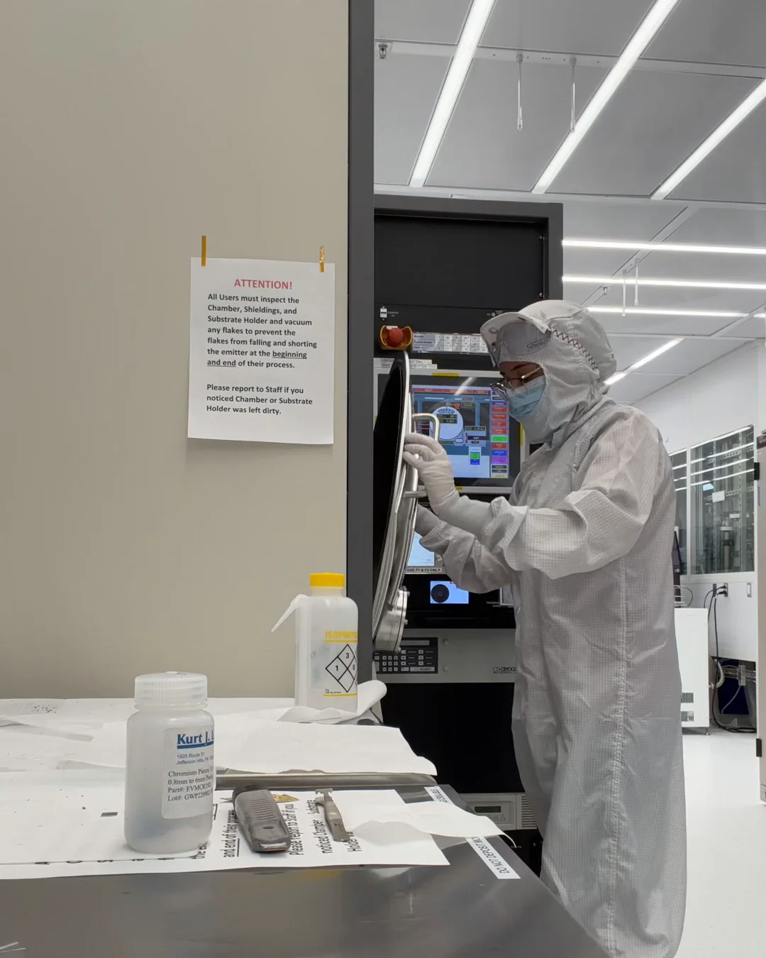
Research internship in USC’s Class 1000 cleanroom. I qualified to run the toolset on my own, ran etch and deposition calibrations that feed the lab’s shared process records, and developed a seed-layer process that keeps high-stress nickel on silicon.
Certifications
IEEE microcredentials in USC nanofabrication, earned through the program’s hands-on training:
- Cleanroom safety and protocols
- Lithography
- Deposition
- Etching
- Metrology
The program
Cleanroom Gateway is run by California DREAMS, one of the Department of Defense’s Microelectronics Commons hubs. It starts with intensive hands-on training in the John O’Brien Nanofabrication Laboratory and continues as a research internship supporting projects in the lab.
My research in the lab supported the Packard Research Group’s spalling work, the wafer-spalling system on the previous sheet. Spalling runs on thin films: a stressed nickel layer, and the seed layer beneath it that has to hold. Learning to make and measure those films here is what let me design the rig around them and debug it when a film was too thin to spall.
Where this work wentPrecision wafer-spalling system
What the program covered
Every process in the lab runs from a written traveler: a step-by-step recipe with the tool, settings and measurements for each step. The curriculum took us through a full device flow, from a bare wafer to a patterned, measured film.
- CleanAcetone, IPA and nitrogen dry at the solvent wet bench.Solvent bench
- PrimeDehydration bake, then HMDS adhesion promoter spun on and baked so resist sticks.Laurell spinner, bake plate
- CoatSpin photoresist to a target thickness and soft bake: AZ 5214E and AZ 1518 (about 2 µm) and AZ P4620 (18 µm thick resist).Laurell spinner, bake plate
- ExposeCalculate exposure time from the measured lamp dose, then contact-print the mask pattern.Karl Süss MJB3 and MA/BA6 mask aligners
- DevelopDevelop, rinse in DI water, dry, and inspect the pattern under the microscope.Developer bench, optical microscope
- DepositGrow and coat films: PECVD oxide and nitride, atomic layer deposition of Al2O3, sputtered and e-beam-evaporated metals, electroplated nickel.Oxford PECVD, Veeco ALD, KJL sputter, CHA e-beam evaporator
- EtchTransfer the pattern: reactive-ion etching of oxide and nitride, ICP etching of III-V semiconductors through oxide and nitride hard masks, and HF wet etching.Oxford RIE 80, Oxford III-V ICP, HF wet bench
- StripRemove resist residue with an oxygen-plasma descum.YES O2 plasma asher
- MeasureFilm thickness, step height and etch depth, then work out deposition rate, etch rate and resist selectivity.Dektak profilometer, Filmetrics F20, ellipsometer
- SingulateDice the finished wafer into individual dies.Dicing saw
Process calibration
The lab keeps a shared calibration log for each tool, so anyone planning a process can work from a measured rate instead of a datasheet number. These are the runs logged under my name, some run alongside lab staff. Each rate comes from film thickness measured before and after, by Filmetrics reflectometry and checked by ellipsometry where noted.
| Tool | Film and recipe | Run | Result |
|---|---|---|---|
| Oxford RIE 80 | SiO₂, standard CHF₃/Ar etch | 5 min, 150 nm removed | 30 nm/min |
| Oxford RIE 80 | SiO₂, standard CHF₃/Ar etch | 6.06 min, 200 nm removed, ellipsometer check | 33 nm/min |
| Oxford RIE 80 | SiNx, standard etch | 5 min, 285 nm removed | 57 nm/min |
| Veeco ALD | Al₂O₃, TMA/H₂O at 150 °C | 500 cycles, 46.4 nm by ellipsometry | 0.93 Å/cycle |
| Veeco ALD | Al₂O₃, TMA/H₂O at 150 °C | 100 cycles, 9.7 nm by ellipsometry | 0.97 Å/cycle |
My two SiO₂ etch runs average 31.5 nm/min, matching the lab’s 31.5 ± 1.0 nm/min across all six SiO₂ calibration runs logged by any operator since May 2026. I also ran a PECVD silicon nitride deposition and measured step heights on patterned wafers with the Dektak.
Victoria: anything you ran that isn’t in these logs (sputtering, e-beam), and what the calibrations were used for.
Measurements
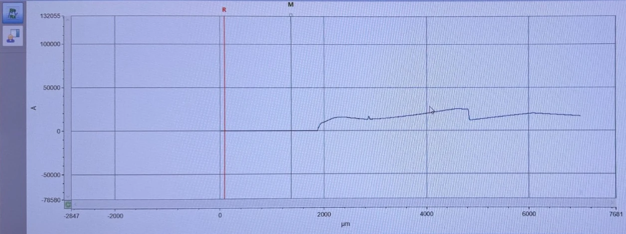
I measure film thickness and step heights on the lab’s Bruker Dektak stylus profilometer. This scan crosses the edge of a plated nickel film from the wafer-spalling work: the profile steps up by about 1.5 µm, the thickness of the plated film.
Seed layer for plated nickel
High-stress electroplated nickel kept failing on silicon: the stress that makes the film useful also pulls it off a weak interface. I developed a Ti/Ni seed layer that held adhesion through 1.4–1.6 µm of high-stress plating and cut failed wafers by 75%.
- Strip the oxideHF dip removes the native SiO₂ so the metal bonds to bare silicon.
- Sputter titaniumA thin Ti adhesion layer bonds to the silicon.
- Evaporate nickelA CHA e-beam Ni seed layer on the titanium.
- Plate nickel1.4–1.6 µm of high-stress Ni electroplated on the seed.
Victoria: layer thicknesses, how the films were failing before, how you measured adhesion, and the wafer counts behind 75%. None of this is in the calibration logs.